Exposure
Exposure
UV lithography is a core technology for precise micro-pattern formation in semiconductor-related manufacturing. UVER’s UV exposure supports futuristic manufacturing process by its high resolution & consistent illuminancy.
Appliable Production Field
PhotoMask
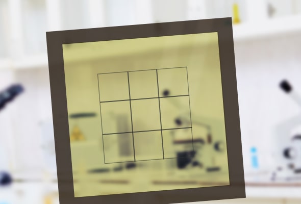
It is an essential semiconductor manufacturing part that operates circuit formation process on semiconductor wafer by using UV light, additionally checking the patterned area on the mask.
Semiconductor
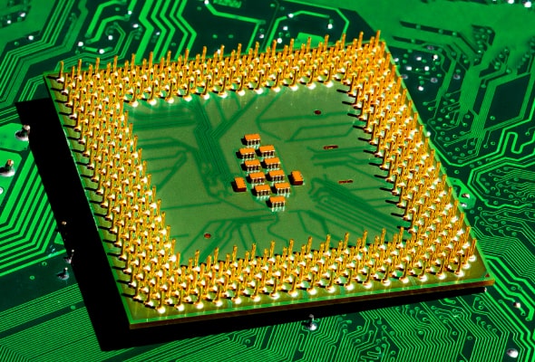
UV exposure technology is mainly used in various semiconductor production parts. It elaborately structures the complicated circuit form inside of the semiconductor chip. By this, computer, mobile phone, tablet and other electronical devices can enhance their overall ability and implement useful functions by the integrated semiconductor chip, and it also contributes the device’s innovation.
Display
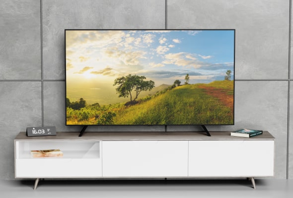
Photolithography creates meticulous circuit pattern in the TFT(Thin-Film-Transiter) device, which is an important semiconductor subpart that adjusts pixel brightness in display monitor. This device plays a significant role in settling the display’s clarity, and UV lithography work is essential for manufacturing those.
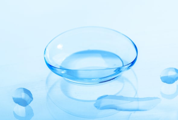
Medical

UV exposure is currently being applied in research & inspections of microorganism, or cell’s microscopic tissue structure and DNA sequencing. It also used in development of medical imaging equipment & medical device as well.
Optical Manufacturing
UV lithography is a necessary technology for manufacturing meticulous optical systems; it serves as a key processing of lens & lens array production, and other qualified optical products.
PCB
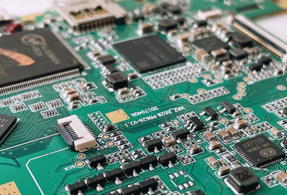
It is used not only in semiconductor manufacturing but also in various industrial fields such as the manufacturing of lasers, optical fibers, LEDs, and PCBs. It plays a crucial role in applications requiring precise image formation, such as the manufacturing of optical components and devices.